Your slogan here
gan substrate
Prior to 1990, we are mentioned possessed condensed matter physics investigation center. In 1990, middle launched Xiamen Powerway Superior Material Co., Limited (PAM-XIAMEN), now it is actually a leading manufacturer associated with compound semiconductor material within China.
PAM-XIAMEN develops superior crystal growth and epitaxy technologies, range from the actual first era Germanium wafer, second creation Gallium Arsenide with base growth as well as epitaxy upon III-V si doped n-type semiconductor components based on Georgia, 's, In, As and also G grown by MBE or even MOCVD, to the 3rd generation: Silicon carbide along with Gallium Nitride for BROUGHT and power device software.
Quality is our very first priority. PAM-XIAMEN has already been ISO9001: 2008 certified in addition to granted honors from Tiongkok General Management of High quality Supervision, Examination and Detachment. We have is the owner of as well as shares four contemporary industrial facilities, which can provide a hefty range of qualified items to satisfy different needs regarding our clients.
Welcome a person to send interrogation in order to our sales team in case you have any more issue. Thank you!
Our Historical past
2011
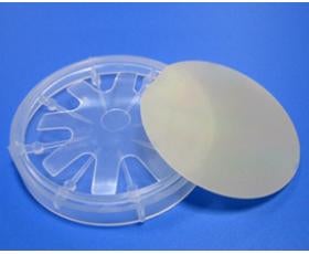
Commercial CdZnTe (CZT) wafer are on bulk creation, which is the new semiconductor, that allows to convert radiation to be able to electron effectively, it will be mainly utilized in infrared thin-film epitaxy substrate, X-ray and also γ-ray detection, laser dvd modulation, high-performance solar tissues and other great areas.
2009
PAM-XIAMEN has built the particular manufacturing technology with regard to GaN epitaxy on Sky-blue along with freestanding GaN solitary amazingly wafer substrate that is regarding UHB-LED and LD. Developed by hydride fumes stage epitaxy (HVPE) technologies, Our own GaN wafer offers lower defect density and fewer or perhaps free macro problem thickness.
2007
PAM-XIAMEN evolves in addition to manufactures compound semiconductor substrates-gallium arsenide crystal as well as wafer. We has used innovative crystal growth technology, up and down gradient freeze (VGF) and also GaAs wafer processing technological innovation, established a production collection from crystal growth, reducing, grinding to polishing running and built a 100-class clean room for wafer cleaning and packaging. The GaAs wafer include 2~6 inch ingot/wafers for GUIDED, LD and Microelectronics programs. Thanks to its efficiency involving molecular beam epitaxy engineering (MBE) and Metallic Natural Chemical Vapor Deposition(MOCVD), the organization can offer globe class epitaxial substance semiconductor wafers for microwaves along with RF applications.
04
PAM-XIAMEN has developed SiC ravenscroft growth technology and Semblable wafer processing technology, set up a production line for you to manufacturer SiC substrate connected with polytype 4H and 6H in different quality levels intended for researcher and business producers, Which is used in GaN epitaxy gadget, power gadgets, high-temperature unit and optoelectronic Devices. Because a professional organization spent by the leading companies from the fields associated with sophisticated and high-tech materials analysis and state study centers in addition to China’s Semiconductor Laboratory, we have been devoted to constantly improve the high quality regarding currently substates as well as create large size substrates, along with epitaxial technology.
2001
gan substrate
PAM-XIAMEN has established production series of semiconductor materials -- Ge(Germanium) Solitary Crystals and also Wafers.
1990
Xiamen Powerway Advanced Materials Co., Ltd(PAM-XIAMEN) founded. PAM-XIAMEN develops enhanced crystal development and epitaxy technologies, production processes, designed substrates along with semiconductor products.
1990 :
gan substrate
We tend to be stated owned reduced issue physics research centre